|
|
|
| iXsenic: a viable alternative
|
|
Evonik has long been focusing on solution-based inorganic materials for the processing of semiconductor, dielectric and passivation layers in TFT backplanes. After intensive research this new material generation is now at a state where it has become a viable alternative to backplane technologies like conventional amorphous silicon (a-Si) or low temperature polysilicon (LTPS).
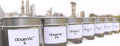
In order to supply the complete package for TFT production from solution and to guarantee convenient one-stop shopping, Evonik is offering a complete range of products for semiconducting, passivation, dielectric and etch-stopping. Inks for Black Matrix applications round out the product portfolio, which is sold under our brand name iXsenic. To provide an optimal fit to the customer's production conditions, the products can be adjusted according to the customer's needs.
Semiconductors
Active matrix-based display technologies of the future require semiconductor materials with a higher performance than a-Si and better upscalability than LTPS. Evonik offers a series of liquid formulations for the solution-based processing of metal oxide semiconductors. These formulations are currently optimized for spin and slot-die coating although any solution-based process is feasible.
Based on current lab results, it is easily possible to drive a backplane unit for LCDs or even OLED displays. Product samples are available as "ready-to-use" formulations in a litre scale and are bottled under cleanroom conditions. |
|
| Related Products |
| 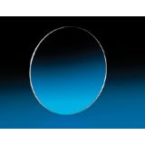 Fused Silica Wafers Fused Silica Wafers
Edmund Optics Inc. (EO)
UV Fused Silica Substrate
Ultrasonically Cleaned
Less than 10Å Surface Roughness
Fused Silica Wafers are thin, circular pieces of UV fused silica ... | |  Silicon Silicon
Jiangxi LDK Solar Hi-Tech Co., Ltd.
Production Technologies
We use metallurgical silicon as a raw material to produce TCS, which is then used to produce polysilicon. This technology enables ... |
|
|
|
|